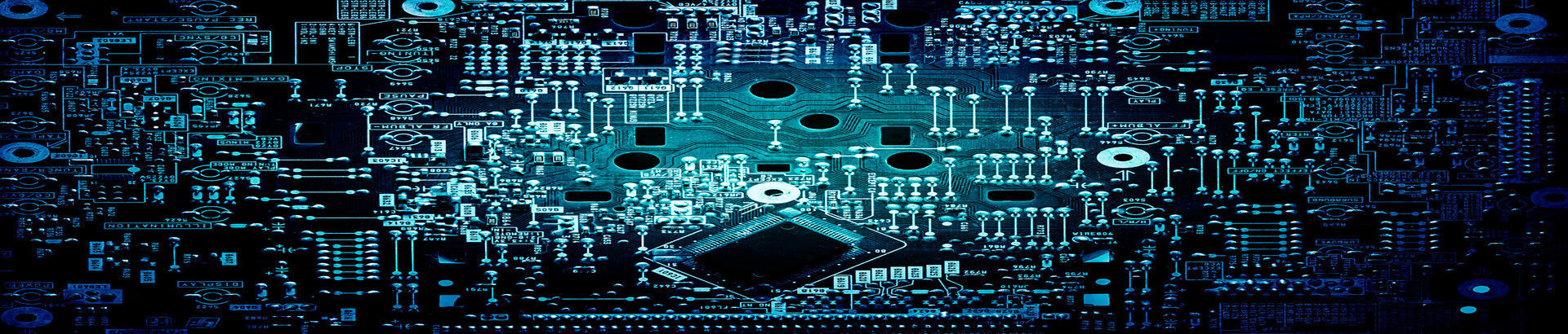
Every time we pick up a smartphone, we experience lightning-fast performance—but we rarely think about the hidden “precision secrets” behind it. One of the unsung technologies supporting the entire semiconductor manufacturing chain is the CNC machine. Every step, from wafer slicing to packaging, demands absolute nanometer-level precision—any tiny error can render an entire chip useless. This is a little-known factor that can determine market leadership.
The Limits of Traditional Manufacturing and the CNC Revolution
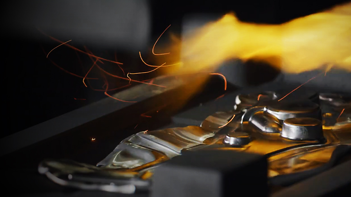
In the early days of semiconductor manufacturing, processes were mostly manual or simple mechanical operations. But as chip line widths shrink to 5 nm or smaller, can these traditional methods keep up? In reality, they often fail due to thermal deformation or vibration, causing surface roughness beyond acceptable limits, ultimately affecting transistor conductivity. This is why CNC machines have become central. Through computer-controlled multi-axis movements, they can achieve sub-micron precision, turning a process from “barely controllable” into near-perfection.
Imagine trying to draw a straight line across the entire Earth, but the error cannot exceed the width of a human hair. That’s the challenge of 0.1 nm precision. In the semiconductor industry, CNC machines bear this responsibility. For example, in manufacturing the lens mounts of extreme ultraviolet (EUV) lithography machines, CNC must handle extremely complex curved surfaces. Without multi-axis synchronized CNC machining, EUV lens mounts would fail under harsh high-temperature and vacuum conditions, causing the entire lithography process to collapse. CNC is the “behind-the-scenes driver” that overcomes this invisible bottleneck, improving chip yield by over 20% and making sub-7 nm processes feasible.
CNC’s Hidden Power in Wafer Packaging
Many people think CNC is just a cutting tool, but it actually combines advanced control systems, modern cutting tools, and intelligent machining strategies. High-precision semiconductor components require multi-axis collaboration and stable structures to maintain both accuracy and efficiency. This not only affects machining quality but also equipment lifespan, operational stability, and the continuous production of chips.
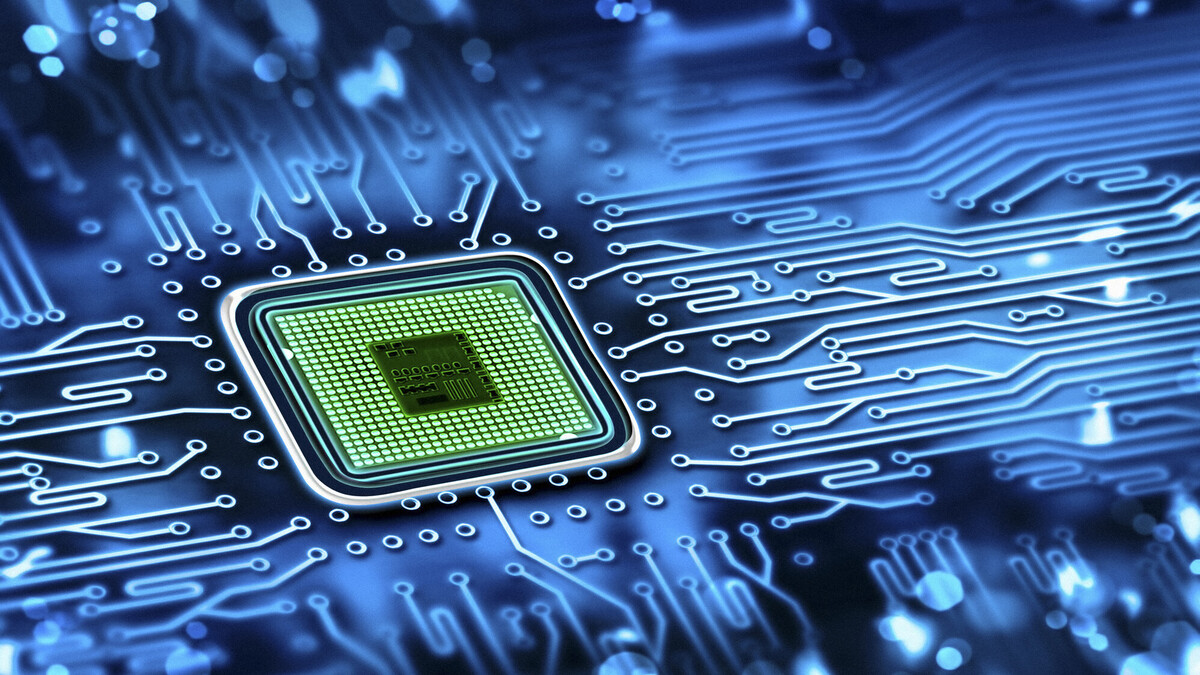
Beyond lithography, CNC plays a key role in semiconductor packaging. Modern chips are moving toward 3D stacking (like TSV technology), requiring precise micro-hole drilling and surface planarization. Intel’s Foveros 3D stacking technology, for instance, requires drilling micro-holes on the wafer with diameters of just 5–10 microns and depth errors controlled within 50 nanometers to ensure seamless signal transmission between chips. Any tiny crack can cause chip failure, making this extremely challenging. CNC machines are critical here. Intel uses Hermle CNC machines from Germany, equipped with high-speed spindles and laser measurement systems, achieving nanometer-level micro-hole machining. The result? Defect rates drop by 25%, machining time is halved, and chips reach the market faster and more reliably.
Semiconductor equipment materials—such as high-hardness alloys, ceramics, or composites—are much harder to process than ordinary metals. CNC machines rely on diverse cutting tools and intelligent cooling systems to machine these materials safely and precisely. Plus, component shapes are often complex, requiring high-precision multi-angle machining. This makes the integration of CNC hardware and software extremely critical.
Conclusion
The semiconductor industry is shifting focus from “shrinking size” to “improving reliability and efficiency,” and CNC machines are at the heart of this transformation. For manufacturers, this is both a challenge and an opportunity to showcase capability. Investing in high-end CNC systems ensures components are flawless at the nanometer scale, helping customers achieve higher yields and faster time-to-market. Ultimately, a chip’s performance lies in the tiniest details—and CNC doesn’t just make parts; it shapes the future of the industry.