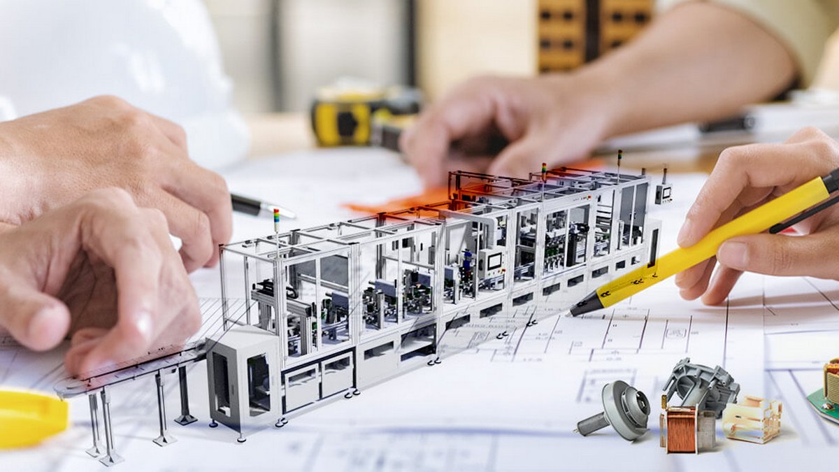
Semiconductors are crucial components in the modern electronics that have revolutionized our daily lives. However, what is often overlooked it that their manufacturing requires a complex integration of unique components such as silicon wafers, dopants, photoresist materials, equipment for lithography, and chemicals for etching. The behind-the-scenes production of semiconductor components involves a complex supply chain, and suppliers of these components play a vital role in semiconductor manufacturing. In this article we will take a look at five of these vital components.
Silicon Wafers: The Foundation of Semiconductor Devices
Silicon wafers serve as the foundational substrate for manufacturing semiconductor devices such as integrated circuits (ICs), microprocessors, and memory chips. Silicon wafers are typically made from high-purity single-crystal or polycrystalline substrates with precise crystalline orientations. Single crystal ingots are pulled from molten material that crystallizes on a base to form a continuous crystal structure. Polycrystalline substrates, on the other hand, are formed by compacting and sintering crystalline powders, resulting in a material with multiple crystal grains.
Single-Crystal and Polycrystalline Substrates
Single-Crystal Substrates are used for high-performance electronics such as integrated circuits (ICs), microprocessors, memory chips, and other high-speed electronic components. In optoelectronic devices such as light-emitting diodes (LEDs), laser diodes, and photodetectors, single-crystal substrates are preferred due to their ability to provide uniformity in quality, which is essential for efficient light emission and detection. They are also commonly used in the production of high-efficiency solar cells where the uniform crystal structure allows for better electron mobility and improved energy conversion efficiency.
Polycrystalline Substrates, on the other hand, are used for low-cost electronics where cost efficiency is a primary consideration. They are used to form the Thin-Film Transistors (TFTs) used in liquid crystal displays (LCDs), organic light-emitting diode (OLED) displays, and other flat-panel technologies. Due to their low cost, they are also widely used in solar panels.
Dopants: Modifying Semiconductor Properties
Once the silicon substrate has been formed, it is sliced into thin wafers via precise sawing or laser cutting, and then polished to a mirror-like finish. The wafers then undergo a doping process, which introduces impurities (e.g., boron, phosphorus) into the silicon substrate to modify its electrical conductivity. Dopants replace silicon atoms in the crystal lattice, introducing extra charge carriers (electrons or holes) and changing the semiconductor's conductivity type (p-type or n-type). Common dopants for silicon include boron (p-type), phosphorus (n-type), arsenic, antimony, and gallium, each with specific doping characteristics and effects on semiconductor performance.
Photoresist Materials: Patterning Semiconductor Layers
Photoresist materials are light-sensitive coatings applied to the surface of silicon wafer substrates to prepare the wafer for the lithography process. These materials are used to define and transfer intricate patterns onto the silicon wafers as they are exposed to ultraviolet (UV) light through a photomask, following the mask design. After the photoresist materials have been applied to the wafer, in subsequent steps, they are illuminated with lithography equipment to form the desired pattern. Etching chemicals will then remove either the illuminated area or the non-illuminated area, depending on the type of photoresist materials used.
There are two main types of photoresist materials: Positive and negative.
Positive photoresists become soluble in developer solutions where they are exposed to light, typically due to a chemical change induced by the exposure. This solubility allows selective removal of the photoresist in the exposed areas, which is often followed by etching or deposition of semiconductor layers.
Negative photoresists become insoluble or resistant to developer solutions where they are exposed to light. This light exposure causes a chemical reaction that makes the resist material harder to dissolve in the developer. As a result, the areas of the substrate covered by the negative photoresist remain protected, allowing subsequent etching or deposition processes to be carried out selectively in the exposed areas.
Lithography Equipment and Pattern Transfer
Lithography defines and transfers patterns onto the photoresist-coated substrates. Lithography equipment uses a mask or reticle with a predefined pattern and a light source or electron beam to transfer the desired patterns onto the photosensitive coating (photoresist) applied to the silicon wafer. After exposure, the lithographic pattern is established, and etching chemicals are employed to selectively remove either the exposed or unexposed areas of photoresist.
Etching Chemicals: Precision Patterning
Etching chemicals, also known as etchants, are used to selectively remove or etch the thin films and patterned layers of photoresist materials from the surface of the wafer based on the pattern defined by lithography, with high precision and accuracy. Etching chemicals are designed with specific etch rates, selectivity, uniformity, and etch profiles suitable for semiconductor materials (e.g., silicon dioxide, silicon nitride, metals). Two methods used are wet etching and dry etching.
Wet etching involves immersing silicon wafers or semiconductor layers in chemical solutions (e.g., acids, bases) that selectively dissolve or remove exposed areas based on chemical reactivity.
Dry etching methods, such as plasma etching (reactive ion etching, plasma-enhanced chemical vapor deposition), use reactive gases (e.g., fluorine, chlorine) and plasma discharges to etch semiconductor materials through chemical reactions and ion bombardment.
As semiconductor technology continues to advance, the complex integration of components used in the industry is sure to witness new applications, materials, and manufacturing processes, and semiconductor components will continue to play a critical role in the design and manufacturing of semiconductors for electronic devices.