What is AOI? AOI stands for automatic optical inspection technology, known for its non-contact nature, rapid speed, high precision, and stability. This technology effectively addresses the limitations of manual visual inspection in quality management.
During the product manufacturing process, various factors contribute to the inevitable production of defects in components. These defects encompass issues like hole dislocation, scratches, open circuits, short circuits, and pollution on printed circuit boards. Additionally, defects such as pinholes, scratches, particles, and mura may be present on the surfaces of the substrate glass and filter of the liquid crystal panel, while the steel strip surface may exhibit cracks, roller marks, holes, and pits. The impact of these defects extends beyond compromising product performance, potentially jeopardizing life safety in severe cases and leading to significant economic losses for users.
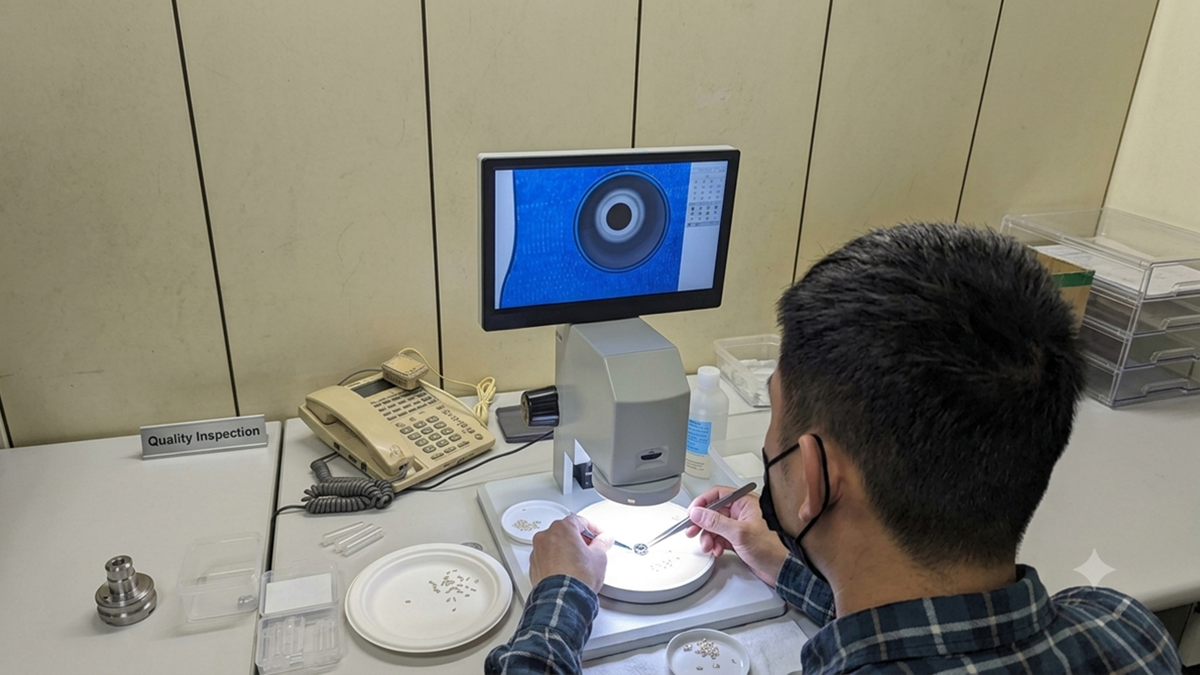
The conventional method for defect detection involves manual visual inspection, a practice still prevalent in industries such as mobile phones, flat panel displays, solar energy, and lithium batteries. However, this method poses challenges, as it requires intense light illumination, causing damage to the eyes of detection personnel. It also suffers from subjectivity, limited human eye spatial and temporal resolution, significant detection uncertainty, and a propensity for ambiguity. These shortcomings, including low efficiency, make it challenging to meet the high-speed and high-resolution detection requirements of modern industry.
With the rapid advancement of electronic technology, image sensing technology, and computer technology, automatic optical (visual) detection technology has emerged as a crucial means of detecting surface defects. This technology, based on optical image sensing, replaces the manual visual detection of surface defects and offers advantages such as automation, non-contact operation, fast speed, high precision, and stability.
What Is AOI?
Automated Optical Inspection (AOI) technology, also known as Machine Vision Inspection (MVI) technology or Automated Visual Inspection (AVI) technology, is widely recognized in industries like flat panel displays, semiconductors, solar, and other manufacturing sectors. While the terms AOI and MVI/AVI are popular, they differ slightly in concept and function.
In a narrow sense, MVI is an emerging scientific technology integrating image sensing, data processing, and motion control for tasks such as measurement, detection, recognition, and guidance in industrial production. MVI uses optical imaging methods to simulate the visual imaging function of the human eye, employing a computer processing system instead of the human brain for data processing. Broadly speaking, MVI expands the functions of human eyes, brains, and hands, focusing on obtaining information from images and feeding it back to automatic actuators to complete specific tasks. Automatic detection technology based on any image sensing method falls under MVI or AVI, with MVI becoming AOI when using optical imaging methods. Thus, AOI can be considered a special case of MVI.
Based on different imaging methods, AOI can be classified into three-dimensional (3D) AOI and two-dimensional (2D) AOI. 3D AOI is mainly used for measuring object shape, geometric parameters, part grouping, positioning, recognition, and robot guidance. On the other hand, 2D AOI is primarily employed for product appearance (color, defects, etc.) detection, classification of different objects or appearances, and distinguishing between good and defective products.
AOI System Composition
Currently, the most widely used AOI system in the industry integrates a simple optical imaging and processing system comprising general devices like cameras, lenses, light sources, and computers. This system, as depicted in Figure 1, captures images directly under the illumination of the light source and processes them using computer algorithms. The advantages of this simple system include low cost, easy integration, and a relatively low technical threshold. It effectively replaces manual detection in the manufacturing process and meets the requirements of most scenarios.
However, for visually inspecting large-format or complex structure objects, single-camera AOI systems may prove insufficient due to limitations in field of view, resolution, accuracy, or specific detection speed requirements. In such cases, the integration of multiple basic units is necessary to collaboratively complete challenging detection tasks. This approach involves adopting a multi-sensor imaging, high-speed distributed processing AOI system integration architecture.
The multi-sensor imaging and high-speed distributed processing MVI system integration architecture serves as a general framework for large-format surface defect AOI detection systems. This system includes components such as a light source, camera array, microscopy re-inspection, cluster parallel processing system, control system, main control computer, server, and an industrial area network interconnected with a factory data center. The system architecture caters to both large-scale surface defect low-resolution rapid detection and high-resolution microscopic re-inspection. The complete AOI system integrates not only the illumination and optical imaging unit but also the test object supporting transmission unit, precision motion mechanism, control unit, and a high-speed parallel image processing unit.
AOI System Integration Technology
AOI system integration technology involves crucial elements such as key devices, system design, machine integration, and software development. Key devices in the AOI system include image sensors (cameras), lenses, light sources, acquisition and preprocessing cards, and computers. Commonly used image sensors comprise various types of CMOS/CCD cameras. The combination of the image sensor, lens, and light source forms the sensing unit in most automatic optical detection systems. Selecting and configuring these devices requires careful consideration of detection requirements.
The choice of a light source involves factors such as color, wavelength, power, lighting method, and needs to consider the image sensor's sensitivity range to the light source spectrum. Lens selection takes into account optical parameters like field of view, depth of field, and resolution. The optical resolution of the lens must align with the spatial resolution of the image sensor for optimal cost performance. In general, the optical resolution of the lens slightly exceeds the spatial resolution of the image sensor. Using a black and white camera for imaging enhances resolution, and the image sensor (camera) adopts area array or line array configurations based on specific requirements. Factors considered when selecting the model include imaging field of view, spatial resolution, minimum exposure time, frame rate, and data bandwidth. Detecting moving objects requires consideration of adverse effects of image motion blur, accurate calculation of the minimum exposure time causing motion blur, and determination of the image sensor type. The exposure time should be less than the minimum causing motion blur, and selecting the global shutter mode is appropriate for fast exposure. Achieving the best signal-to-noise ratio involves maximizing the image sensor gain, improving image brightness with the light source's energy (power), or increasing the lens aperture diaphragm without affecting the available imaging depth of field.
In system integration, designing the support method and precision transmission and positioning device for the device under test is crucial. This involves precision mechanical design technology, which is vital in automatic manufacturing and assembly industries such as flat panel displays, silicon wafers, semiconductors, and MEMS. The optical inspection system in these fields operates in ultra-clean rooms, necessitating a high self-cleaning ability. System component materials, pneumatic and automatic device selection, motion guide design, and device selection all have strict requirements to prevent secondary pollution to the production environment, particularly the workpiece itself. For online inspection of large parts (e.g., high-generation liquid crystal glass substrates, silicon wafers), adopting air float support, positioning and transmission mechanisms, self-lubricating devices for moving parts (e.g., bearings), FFU fans for environmental purification, and static elimination devices for anti-static treatment on the workpiece are often necessary.
High-speed image data processing and software development stand out as core technologies in automatic optical inspection. Since automatic optical detection relies on image sensing to obtain measurement information, data amounts can be substantial, especially in high-speed online detection where image data can be massive. To meet production beat requirements, high-speed data processing technology is essential. Common methods include shared memory multi-thread processing, shared memory or distributed memory multi-process processing, and using distributed computer clusters to divide huge images into small data streams processed by individual cluster nodes. For time-consuming and complex algorithms, achieving time requirements may be challenging with only the computer CPU. Hardware processing technologies such as DSP, GPU, FPGA, and other hardware processing modules may be required to work in conjunction with the CPU for fast and complex calculations.
In Summary
In recent years, especially since the introduction of China's "Made in China 2025" development strategy in 2015, the replacement of people with machines—specifically using machine vision or automatic optical inspection instead of human vision—has gained traction. This shift has enabled efficient and online automatic inspection and quality control of product parts manufacturing quality, garnering favor across industries. AOI technology is now widespread in sectors like industry, agriculture, and biomedicine, particularly in precision manufacturing and assembly industries such as mobile phones, liquid crystal panels, silicon wafers, and printed circuit boards. Notably, the development of 3D AOI for assembly guidance and 2D AOI for surface defect detection continues to progress with the emergence of advanced inspection equipment.