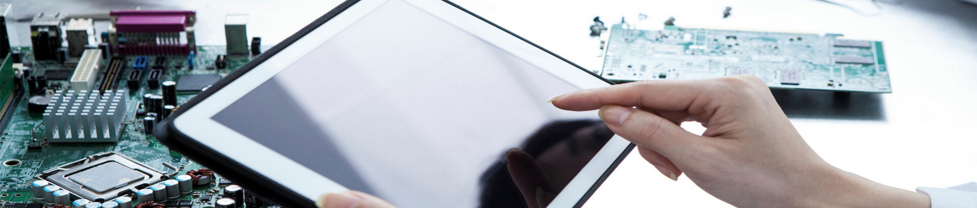
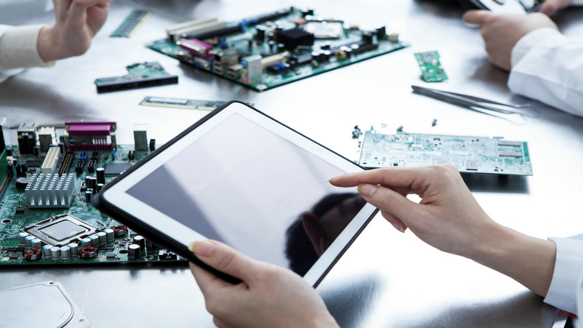
The Printed Circuit Board (PCB) is one of the main parts of all electronic products. The application fields of PCB are quite extensive. Wherever electronic components are used, PCBs are almost always used. Currently, they are mainly used in the fields of information, communication, consumer products, automobiles, aerospace and military, precision instruments and industrial products. They are an indispensable basic part of all electronic products. This article will be divided into several aspects to discuss PCBs, namely type, material, process, installation and welding. Let us have a good understanding of the "mother of the electronics industry" – the PCB.
What is a Printed Circuit Board, PCB?
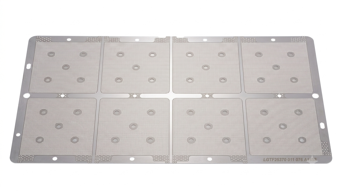
A PCB is a complex circuit of copper etched on a board. It is the main support body for electronic components during installation and interconnection. It is used as the foundation for fixing electronic components into a circuit, and providing electric currents between these components. As an indispensable basic part of all electronic products, the PCB is known as the "mother of the electronic industry".
- Upstream is glass fiber, copper foil, resin and other materials.
- Midstream is Copper Clad Laminate (CCL) a copper foil substrate printed on the circuit board.
- Downstream is all kinds of electronic products
Without the PCB, the efficacy of electronic products cannot be reached. Although the PCB industry is a mature industry, it continues to play an important basic role in the electronic technology industry.
The application fields of PCBs are quite extensive. Wherever electronic components are used, PCBs are almost always used. Currently, they are mainly used in the fields of information, communication, consumer products, automobiles, aerospace and military, precision instruments and industrial products. According to the application fields, PCBs can be divided into single-sided, double-sided, four-layer and more multi-layer boards and flexible boards. Generally speaking, the more complex the functions of electronic products, the longer the circuit distance, the more contact pins, and the more layers required for the PCB, such as high-end consumer electronics, information and communication products, etc.
At present, the mobile phone industry that uses PCBs in bulk is experiencing a slowdown in growth, but with the continuous improvement of specifications, 5G commercial transfer, servers, a large number of small base stations, and storage devices, etc., will be the next terminal products to use PCBs. The material requirements have also begun to move towards high-speed, high-frequency, and high-density packaging. The Electric vehicle industry is also another new industry which is driving PCB growth, causing the average selling price of PCBs to continue to rise in recent years.
What is a Printed Circuit Board, PCB?
All electronic products must use "Printed Circuit Boards" to fix integrated circuits (ICs) and other electronic components (such as resistors, capacitors, inductors.) Different integrated circuits and electronic components are connected by thin copper wires to provide a stable working environment, so that electronic signals can flow between different electronic components.
Types of Printed Circuit Boards
- Single sided board: A single plastic board is used as the bottom plate, integrated circuits (IC) and other electronic components are concentrated on one side, and copper wires are concentrated on the other side. The number of copper conductors that can be made on a single panel is small, and only early circuit boards will use this layout.
- Double sided board: Using a single piece of plastic board as the bottom plate, copper wires are made on the front and back surfaces of the bottom plate, and "vias" are drilled to allow the copper wires to pass through the plastic board from the front to the back, to connect the copper wires on the front and back surfaces to each other. This layout is used for more complicated circuits.
- Multilayer board: Multiple double-sided boards are sandwiched with an insulating layer (plastic material) between the double-sided boards. Multiple layers of copper wires form complex circuits. At present, the motherboards used in computers are mostly limited to eight-layer boards because of the limited number of components.
Generally, small electronic products, such as mobile phones, tablet computers, etc. use boards with at least eight layers, due to the requirement of small size. Smaller products with more electronic components will usually require more layers of circuit boards.
"Via" is generally used in double-sided boards to drill holes through the plastic board, but in multi-layer boards, if you only want to connect some internal circuits, it is not necessary to penetrate the entire plastic board. You can use "via”, “buried via hole" or "blind via hole" when it is only necessary to penetrate a few layers of the plastic board.
Printed Circuit Board Materials
- Rigid printed circuit board (RPCB): Generally made of glass epoxy resin (glass epoxy), a hard plastic board, with copper wires printed on the circuit board. The greatest feature of the rigid circuit board is that it is "inactive." Because it is hard, it can only be fixed in the casing after it is made. It is the circuit board that is currently most used in all electronic products.
- Flexible circuit board (FPCB): Generally made of polyethylene terephthalate (PET) or Polyimide, with copper wires printed on the circuit board. The major feature of the flexible circuit board is that it can bend. The soft PET material is the same material used to make carbonated beverage bottles. It can be bent into various shapes after production is completed. They are widely used in consumer electronic products, such as LCD screens of notebook computers, foldable mobile phones, digital Cameras, CD players, hard disk storage devices, etc.
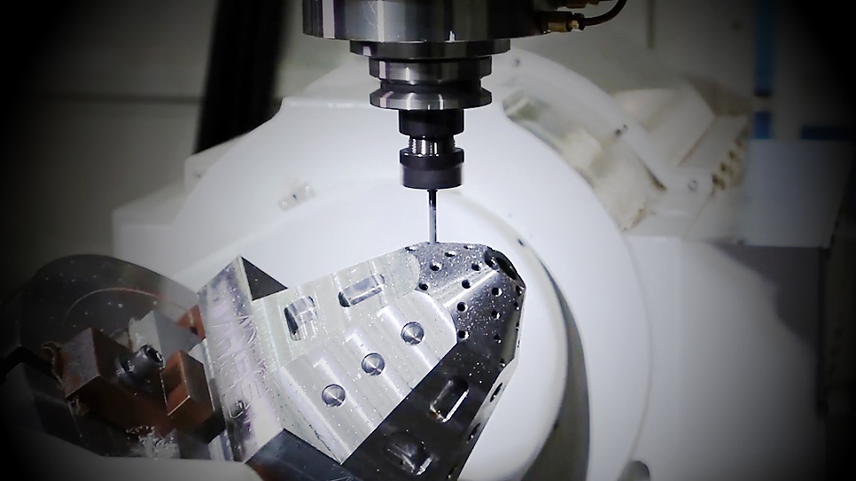
Printed Circuit Board Production Processes
The production processes of printed circuit boards include: single-sided production, drilling and electroplating, multi-layer printed circuit board bonding, protection and surface treatment, circuit testing, etc. The details are as follows:
- Single-sided production: The designed circuit is made into a negative and then transferred from the negative to a thin layer of copper foil. Unnecessary copper foil is dissolve with chemicals leaving only the needed circuit. This process is a bit similar to transferring the pattern on a photomask to the silicon wafer in a fab. If a double-sided board is produced, copper foil will be applied to both sides of the plastic board. If a multi-layer board is produced, many double-sided panels are glued together.
- Drilling and electroplating: To make double-sided or multi-layer boards, via holes, buried via holes, or blind via holes are first made in the board. The minimum size of the hole that can be drilled using a mechanical drill is 8mil (about 0.2mm) but a laser drill, using laser light, can be used to penetrate the plastic plate to make a hole as small as 4mil (about 0.2mm) or less. A process called HDI (High Density Interconnection) uses thinner and denser copper wires to reduce the size of the integrated circuit (IC) and other electronic components of the circuit board. After drilling is completed, a layer of metal is plated into the holes to form vertical copper wires. “Via" is sometimes referred to as "PTH: Plated Through Hole".
- Multilayer printed circuit board bonding: The fabricated double-sided boards are bonded to form a multi-layer board. When bonding, an insulating layer (plastic material) must be added between the layers. If there are perforations (via) that penetrate several layers, then each layer must repeat the above steps. The circuits on the front and back surfaces of the multi-layer board are usually fabricated after the multi-layer board is bonded.
- Protection and surface treatment: The green or brown on the printed circuit board is the color of the "solder mask". The solder mask is an insulating protective layer, which can protect the copper wires from oxidation. A layer of "silk screen" will have text and symbols printed on it to indicate the names and positions of various integrated circuits (ICs) and other electronic components.
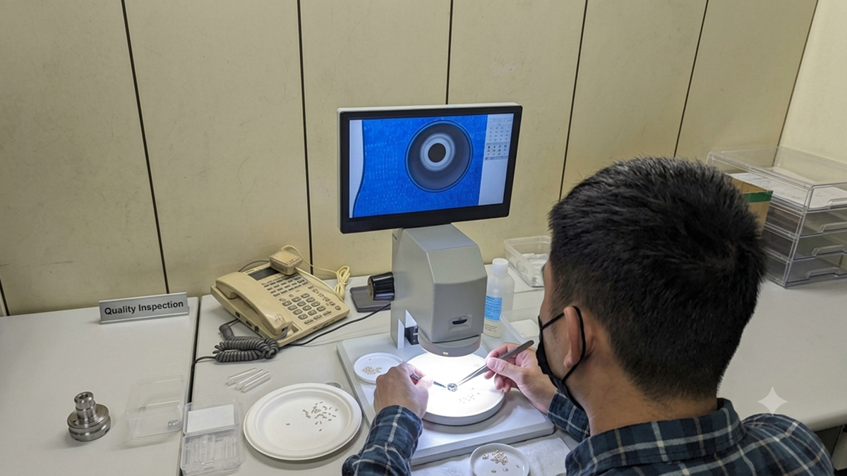
- Line test: This is a test used to determine whether there is a short circuit or open circuit on the printed circuit board. Generally, the board can be scanned optically with infrared light to find out the defects of each layer, and whether there is an incorrect gap between the wires. An electronic testing method called "flying probe” can also be used to check all copper wire connections for shorts or open circuits.
Component Mounting and Soldering Technology
After the printed circuit board is completed, the integrated circuit (IC) and other electronic components must be connected and fixed on the printed circuit board.
- Through Hole Technology (THT): Electronic components are placed on the front of the circuit board, and the pins are soldered on the back, usually using "wave soldering" technology. Pins are first cut close to the board and bent slightly so that the components can be fixed in place. Then the bottom of the board is coated with a flux to remove the oxide on the bottom pins. The board is reheated to remove any melted solder, and after cooling, the connection is fixed. This method will take up a lot of space, and a hole needs to be drilled for each pin, as each pin occupies space on both sides of the circuit board. The solder joints are relatively large, but the fixing effect is better.
- Surface Mounted Technology (SMT): Electronic components and pins are placed on the front of the circuit board, usually using "over reflow soldering" technology. Solder paste containing flux and solder is first printed on the circuit board where it is to be connected to the pins of the electronic components. Then the electronic components are placed on the circuit board so that the pins are in contact with the solder paste on the circuit board. The circuit board is then heated to melt the solder paste and bond the pins of the electronic components. When the solder cools down, the electronic component pins will be fixed on the circuit board. The electronic components soldered in this way are relatively small in size, and the electronic components are denser on the circuit board. Most current electronic products use SMT technology instead of THT technology.