The Foundation of the Semiconductor Industry: What is A Wafer?
Knowledge

The Foundation of the Semiconductor Industry: What is A Wafer?

In the semiconductor news, wafers are always mentioned in terms of dimensions, such as 8-inch or 12-inch wafers, but what exactly is a so-called wafer? What does the 8 inches refer to? How difficult is it to produce large-sized wafers? The following is a step-by-step introduction to the most important foundation of semiconductors - what is a "wafer".
Published: Aug 25, 2022
The Foundation of the Semiconductor Industry: What is A Wafer?

What is A Wafer?

Wafers are the basis for the manufacture of various computer chips. We can compare chip manufacturing to building a house with Lego blocks, and by stacking layer by layer, we can complete our desired shape (that is, all kinds of chips). However, if there is no good foundation, the built house will be crooked and unsatisfactory. In order to make a perfect house, a stable base plate is required. For wafer fabrication, this substrate is the wafer described next.

First of all, recall that when I was a child with Lego blocks, there would be a small round protrusion on the surface of the blocks. With this structure, we can stably stack the two blocks together without using glue. Wafer fabrication, in a similar way, holds the subsequently added atoms together with the substrate. Therefore, we need to find substrates with neat surfaces to meet the conditions required for subsequent fabrication.

In solid materials, there is a special crystal structure - Monocrystalline. It has the property of atoms closely arranged one after the other, which can form a flat atomic surface. Therefore, using a single crystal to make a wafer can meet the above requirements. However, how to produce such a material, there are mainly two steps, namely purification and crystal pulling, after which such a material can be completed.

How To Make a Single Crystal Wafer

The purification is divided into two stages. The first step is metallurgical purification. This process is mainly to add carbon to convert silicon oxide into silicon with a purity of more than 98% by means of redox. Most of the refining of metals, such as iron or copper, is done in this way to obtain metals of sufficient purity. However, 98% is still not enough for wafer manufacturing and still needs to be improved further. Therefore, the Siemens process will be used for further purification, so that the high-purity polysilicon required for the semiconductor process will be obtained.

Next, is the step of pulling crystals. First, the previously obtained high-purity polysilicon is melted to form liquid silicon. After that, the single-crystal silicon seed contacts the liquid surface, and slowly pulls up while rotating. As for why single-crystal silicon seeds are needed, it is because silicon atoms are arranged in the same way as people line up, and they will need to be in the front line to let later people how to arrange them correctly. Finally, after the silicon atoms leaving the liquid surface solidify, the neatly arranged monocrystalline silicon pillars are completed.

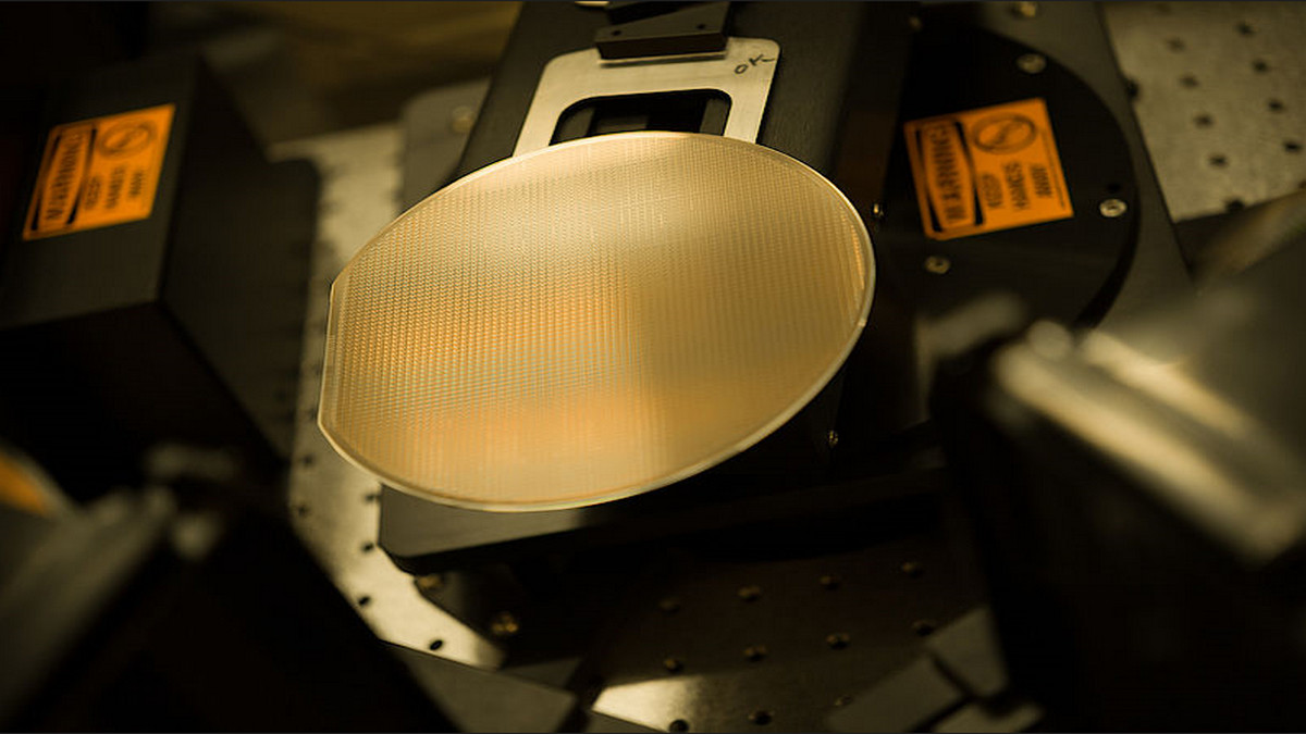
However, what do 8 inches and 12 inches stand for? In fact, it refers to the crystal column. How difficult is it to make large wafers? As mentioned earlier, the production process of the crystal column is like making marshmallows, and it is formed while rotating. Anyone who has made marshmallows should know that it is quite difficult to make large and solid marshmallows, and the process of pulling crystals is the same. The speed of rotation and temperature control will affect the quality of the crystal column. Therefore, the larger the size, the higher the speed and temperature requirements for crystal pulling, so it is more difficult to make high-quality 12-inch wafers than 8-inch wafers.

However, an entire silicon pillar cannot be used as a substrate for wafer fabrication. In order to generate silicon wafers one by one, a diamond knife is used to cut the silicon pillars laterally into wafers, and the wafers can be polished to form wafers. Fabricate the required silicon wafers. After so many steps, the fabrication of the wafer substrate is complete, and the next step is the step of stacking the house, which is wafer fabrication.

Published by Aug 25, 2022 Source :Business Next

Further reading

You might also be interested in ...

Headline
Knowledge
Essential for Precision Machining: A Complete Guide to Tungsten Carbide Center Drills
In modern manufacturing, precision is the core standard by which product quality and performance are measured. From aerospace components to medical devices, even a minor deviation can lead to serious consequences. When it comes to precision drilling, a critical challenge is ensuring that a drill bit can be accurately positioned at the start of a cut while maintaining stability during high-intensity operations. The tungsten carbide center drill is the professional tool engineered specifically to solve this problem.
Headline
Knowledge
From Cavitation Effect to Industrial Applications: The Secrets of Ultrasonic Cleaning
When your glasses, tableware, or electronic components are stained with stubborn dirt, what can you do? Traditional methods often require vigorous scrubbing or even harsh chemical solvents, which are not environmentally friendly and may scratch the item. At this moment, ultrasonic cleaning acts like an “invisible little helper”, reaching deep into grooves and gaps to gently yet effectively remove contaminants.
Headline
Knowledge
The “Spark Magician” of Metalworking
Electrical Discharge Machining (EDM) is a non-traditional machining process that removes metal through electrical sparks. Unlike conventional methods, it is not limited by material hardness and can precisely create deep cavities, micro-holes, and complex structures in hardened steel, tungsten carbide, or superalloys. The three main types of EDM include wire cutting, die-sinking, and hole drilling, which are widely applied in mold making, aerospace, automotive, and medical industries. Although EDM has a slower processing speed, works only with conductive materials, and requires consideration of electrode wear and surface treatment, its advantages in high precision, zero cutting force, and superior surface finish make it an indispensable technology in precision manufacturing. Moreover, it continues to evolve in line with the trend toward smart manufacturing.
Headline
Knowledge
Press Brake vs Shearing Machine: Functional and Technical Comparison of Industrial Processing Equipment
Press Brake and Shearing Machine are two essential types of equipment in the field of machine tools, widely used in the processing of metal, wood, and other materials. They play critical roles in manufacturing, enabling efficient and precise material forming and cutting. This article introduces the definitions, functions, technical features, and applications of folding and cutting machines, offering neutral and practical knowledge sharing.
Headline
Knowledge
Master Chuck Types & Selection: The Essential Guide for Machinists
In the world of precision manufacturing, every minute detail can determine the quality of the final product. The chuck is a critical yet often overlooked component—it's not just a tool for holding a workpiece, but the very heart of ensuring machining accuracy, efficiency, and safety. This article will take you on a deep dive into the diverse universe of chucks, covering their operating principles, design philosophies, common types, and how to select the right jaws and chucks for different needs. Whether you're new to the industry or a seasoned engineer, this guide will unlock the intricate secrets of chucks, helping you master every detail on your path to manufacturing success.
Headline
Knowledge
An Overview of Electrical Discharge Machining (EDM)
Electrical Discharge Machining (EDM) is a non-traditional manufacturing process that utilizes electrical sparks to remove material from a workpiece. Unlike conventional machining methods such as milling or turning, which rely on physical contact between a tool and the material, EDM operates without direct contact, making it ideal for processing hard or brittle materials that are difficult to machine otherwise. The process involves generating a series of rapid electrical discharges between an electrode and the workpiece, submerged in a dielectric fluid, which erodes the material through thermal energy. This technique has revolutionized precision manufacturing by enabling the creation of complex geometries with high accuracy.
Headline
Knowledge
Applications of Machine Tools in the Aerospace Industry
The aerospace industry is a highly specialized and technology-driven sector, encompassing the design, manufacturing, and maintenance of aircraft, spacecraft, satellites, and related equipment. Machine tools play a critical role in this field, enabling the precision machining of complex metal and composite material components. These tools enhance production efficiency while ensuring the accuracy and reliability required to meet the stringent safety and performance standards of aerospace. This document outlines the key applications, technologies, benefits, and future trends of machine tools in the aerospace industry.
Headline
Knowledge
Smart Healthcare Uncovered:How AI Is Transforming Clinical Practice?
With the rapid rise of artificial intelligence (AI), the healthcare industry is undergoing a disruptive transformation. AI is significantly improving diagnostic accuracy and treatment efficiency while profoundly redefining healthcare professionals’ roles and patient experiences. A comprehensive understanding of the core technologies and clinical applications behind this transformation is essential for grasping the future trends and strategic directions of smart healthcare.
Headline
Knowledge
Principle and Applications of Laser Cutting Machines
As the global manufacturing industry advances toward higher precision and efficiency, laser cutting technology has become a key enabler of industrial upgrading. Compared with traditional shearing, stamping, and mechanical cutting, laser cutting offers non-contact processing, higher accuracy, and greater flexibility. It significantly improves productivity while reducing secondary finishing. Today, it is widely adopted in metalworking and increasingly applied in electronics, aerospace, medical, and architectural design industries.
Headline
Knowledge
Why Are High-Quality Cutting Fluids Critical for Machining Quality?
In CNC and metalworking, cutting fluid is no longer just a coolant—it plays a critical role by providing lubrication, chip removal, and corrosion protection. With the right formulation and concentration, it can reduce cutting heat, minimize friction, extend tool life, and maintain workpiece accuracy. High-pressure cooling further enhances efficiency in deep-hole and high-speed machining. The pairing of tool material with the proper cutting fluid is equally crucial; correct selection and maintenance ensure process stability, prolong equipment life, and improve the overall work environment. Cutting fluid has become an indispensable investment in modern precision manufacturing.
Headline
Knowledge
Introduction to Emerging Printing Technologies: Opening New Horizons for the Future of Printing
With rapid technological progress and increasingly diverse market demands, traditional printing techniques are no longer sufficient to meet modern industry’s requirements for precision, efficiency, and sustainability. As a result, emerging technologies such as UV printing, 3D printing, and Nanoimprint Lithography (NIL) have risen to prominence, offering solutions with higher precision, broader applications, and lower production costs. These innovations have already demonstrated value across packaging, advertising, healthcare, semiconductors, and construction. In the following sections, we will explore their technical features and real-world applications, highlighting the advantages and future potential of these cutting-edge printing technologies.
Headline
Knowledge
The Core Standard for Life-Critical Systems: A Complete Guide to IPC Classification
In high-risk fields such as medical, aerospace, and automotive, IPC classifications determine PCB reliability and safety. Class 3 represents the highest standard, requiring zero tolerance for defects, complete via filling, adequate copper annular rings, and rigorous inspections to ensure operation under extreme conditions, while Class 2 suits long-term use in non-critical equipment with minor cosmetic flaws allowed. Class 3’s strict criteria cover component placement, soldering, plating thickness, and environmental testing—adding cost and production time, but far outweighing the risks of failure in life- or safety-critical systems. Thus, defining high-risk equipment as Class 3 during design is essential, making IPC classification a core safeguard rather than an option.
Agree