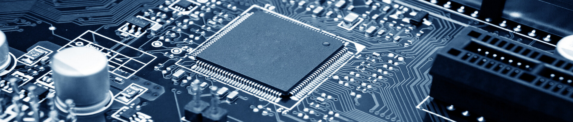
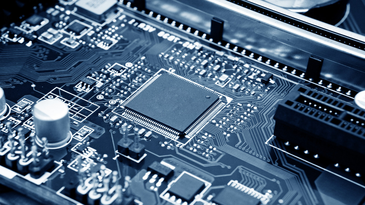
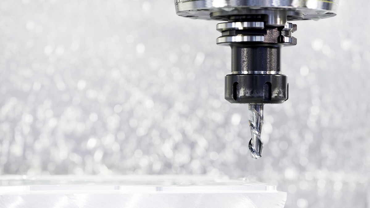
Wafer-level packaging (WLP) has gained traction over the past decade as the semiconductor industry continues to push for generations of higher-performance chips. Back-end packaging technologies are becoming increasingly important in meeting the demands of low-latency, high-bandwidth, and low-cost semiconductor devices.
Global Semiconductor Packaging Materials Market Outlook:
The ever-changing semiconductor process technology has resulted in many new products and applications. Moreover, 5G communication technology has three main advantages large connection, ultra-high speed, and low latency, which makes the semiconductor industry even more powerful. It is estimated that 5G new technology will simultaneously drive global epidemic prevention. The demand for applications such as technology, smart home, smart manufacturing, smart medical care, and automotive electronics continues to increase. At the same time, to meet the requirements of continuous miniaturization and functional diversification of electronic products, the demand for chip integration is increasing day by day. Not only the process side continues to improve the resolution of chip circuits but also achieves higher density circuit layouts to reduce product volume. The continuous evolution of packaging technology is also a great help, and the performance of packaging materials will be one of the key focuses. In recent years, packaging materials have continued to move towards features such as low dielectric loss (Low Df) and filler (Filler) particle size miniaturization. Developed to support evolving chip packaging needs.
In response to the need for miniaturization, multi-function, and shortened development cycle of electronic components, the proportion of advanced packaging in the semiconductor industry has steadily increased. The compound annual growth rate of the traditional packaging market is only 2.4%. To seize the technological high ground, the world's major packaging and testing factories, fabs, and IDMs are stepping up their deployment of advanced packaging.
According to the forecast of the global semiconductor packaging materials market outlook report, the global semiconductor packaging materials market will follow the growth of the chip industry, with market revenue rising from US$17.6 billion in 2019 to US$20.8 billion in 2024 (CAGR of 3.4%). It is the various new technologies that drive the semiconductor industry behind this wave of gains, including big data, high-performance computing (HPC), artificial intelligence (AI), edge computing, advanced memory, 5G infrastructure expansion, 5G smart adoption of mobile phones, growth in the use of electric vehicles, and enhanced car safety features, among others. Packaging materials are the key to the continued growth of advanced technology applications, supporting cutting-edge packaging technologies and enabling a new generation of chips that combine high performance, reliability, and integration.
In addition to system-in-package, wafer-level packaging and 3D packaging are also the main trends in the development of the packaging industry. The FLIP-CHIP share is expected to drop to around 70% by 2024. Over the next five years, the fastest-growing technologies for the advanced packaging market are expected to be fan-out packaging and silicon vias. Most industry players remain optimistic about the growth of fan-out packaging, believing that productivity will rise from current levels.
Laminate Substrate of packaging materials, due to the increasing demand for system-in-package (SIP) and high-performance devices, the compound annual growth rate of laminate substrate will exceed 5%. And the 9% CAGR for wafer-level packaging (WLP) dielectrics will be the fastest during the forecast period. Although various new technologies to improve performance are being developed, the development trend of pursuing smaller and thinner packages will be a drag on the growth of the market for lead frames, die to attach, and encapsulants.
What is Semiconductor Packaging?
After circuits are etched from the wafer and cut into independent dies, one or several dies are assembled or potted into a semiconductor package in the integrated circuit packaging stage. Semiconductor packaging provides a certain degree of impact/scratch protection for the die, provides pins or contacts for the die to connect with external circuits, and helps to take away the heat generated by the die when the die is working. Nowadays, there are many kinds of packaging of semiconductor components and integrated circuits. Many of them are industry standards for semiconductors, while others are special specifications of a component or integrated circuit manufacturers.
A semiconductor package has at least two pins or contacts to connect to one end of the circuit. An example of such a component is a diode. If the packaged die is a microprocessor-type integrated circuit, then packages for this die need to provide hundreds or even thousands of contacts or pins. Some small semiconductor packages are typically bonded to external circuits with contacts or thin leads. For some larger integrated circuits and some high-power semiconductor components, especially in applications that require more high-power power consumption, it is necessary to pay attention to the thermal conductivity and heat dissipation capacity of the package, to take away the heat generated by these chips during operation waste heat.
In addition to providing the ability to connect and conduct heat and heat dissipation for the packaged semiconductor die, the semiconductor package must protect the die from the outside world, for example, the infiltration of moisture is not allowed. Free particles or corrosion inside the package will greatly reduce or even damage the performance of semiconductor components and integrated circuits. Some die also requires the semiconductor package to provide sealing, no gas and liquid exchange with the external environment, etc., and glass, ceramic, or metal is generally used as the packaging material.
With the steady advancement of semiconductor packaging technology innovation, areas with greater market opportunities for materials in the next few years include the following:
- New substrate designs that support higher density and narrow bump pitches.
- Low dielectric constant (DK) and dielectric loss (DF) laminates for 5G mm Wave applications.
- The coreless structure is based on a modified version of the lead frame technology, that is, a pre-packaged interconnect system (MIS).
- Provide underfill for copper pillar flip chip package with molding compound.
- Smaller fillers and narrower particle size distributions are required to handle narrow gap and fine pitch flip chip resin materials.
- Low-to-no resin bleed, no-to-low outgassing, and sticky-grained materials for placement processes below 5 micrometers (µm).
- Lower dielectric loss (DF) dielectrics are required for higher spectrum applications such as 5G.
- Void-free deposition and low-coverage deposition for through-silicon (TSV) plating.
Semiconductor packaging materials include the following:
- Substrates
- Lead frames
- Bonding wire
- Encapsulants
- Underfill materials
- Die attach
- Solder balls
- Wafer-level package dielectrics
- Wafer-level plating chemicals
Types of Conductor Molding Materials:
- Solid state molding compound:
Epoxy Molding Compound (EMC) is mainly composed of epoxy resin, phenolic resin, catalyst, silica powder, etc. It is the earliest and most mature type of epoxy molding compound.
There are two molding methods for solid molding materials, including Transfer Molding and Compression Molding. Among them, the transfer molding process is used for molding, which is the most used in semiconductor packaging materials. This material is almost used in packaging from traditional lead frame packaging to BGA packaging. If it is applied to a large area of wafer level for encapsulation, granule molding compound (GMC) is applied evenly and then the compression molding process is used for encapsulation.
Epoxy molding resin is also the most common solid-state molding material, which is composed of epoxy resin (5~10wt%), hardener (5~10wt%), catalyst, and inorganic filler, coupling agent, flame retardant, release agent. It is composed of mold agents and pigments, among which the inorganic filler silica (60~90wt%) accounts for the largest proportion. The size of spherical silica is important. Large size can easily cause voids. If ultra-small fillers are used, attention should be paid to the problem of dust generated during the process, which will also cause inconvenience in cleaning. At the same time, the Filler material will also affect the overall molding material. Although the epoxy resin material only accounts for 5~10wt%, its low warpage performance can improve the reliability of the overall assembled product, and is the most important material to determine the product and processing properties. Solid-state molding materials are used in general IC packaging, such as TSOP, DIP, QFN, Dual QFN, QFP, BGA, etc. In recent years, it has been used in large-area packaging.
- Liquid packaging material:
The most important uses of liquid packaging materials are COB (Chip on board), underfill, tape-and-reel TCP/COF substrate, and wafer bonding and filling to protect bonding points. In addition, liquid molding compound (LMC) for the fan-out wafer-level package is the mainstream material currently used in the market, and the compression molding process is directly used for packaging.
The ACF (An-isotropic Conductive Film) material itself is uniformly distributed in the organic resin material by a certain amount of conductive powder and exists in the form of a B-STAGE film by coating. When the ACF is attached between the bumps on the IC surface and the substrate circuit using the thermo-compression bonding process, using appropriate pressure, time, and temperature, the conductive adhesive starts to flow, and the conductive powder contacts the bumps and the substrate circuit, and then To achieve the effect of electrical conduction, at the same time, the appropriate particle size and addition amount of the conductive powder make it impossible to contact each other between the bumps and achieve the characteristics of anisotropic conduction. ACF mainly uses the thermo-compression bonding process to bond the driver IC and the substrate.
Chip packaging materials are large-area packaging materials developed for the development trend of WLP and PLP wafer-level packaging in recent years, which can achieve complete attachment. A new material that does not cause dust problems. In future large-area packaging, sheet-like films and granular materials are mainly used, and the thickness of sheet-like films can be controlled to be about 200 μm or even thinner. At present, the thin packaging of 12-inch wafers mainly uses liquid packaging materials.
Global Packaging Materials Market Analysis:
The COVID-19 epidemic broke out in early 2020, and the epidemic began to spread around the world in the second quarter, which made the semiconductor market hesitate to assess the year-on-year growth of global semiconductor demand. The demand for materials has declined, but starting from the second half of 2020, the overall market has brought about the demand for remote technology due to the epidemic. Which has increased the demand for home epidemic prevention and zero-contact, such as homework, distance teaching, and home economics. Which has led to the improvement of terminal products (NB, tablets, game consoles), and NetCom equipment (servers, SSDs, network switches) has increased sales, coupled with the gradual maturity of 5G technology and the growth in the number of terminal device demand, the global demand for packaging materials has not decreased but increased.
Therefore, the future growth momentum of packaging materials will mainly come from automotive electronics, automotive ECUs, and 5 G-related application modules. Among them, MUF materials are mainly used in AP (Application Processor) and BB (Baseband Processors) packaging. In the future, MUF materials will increase due to the increase in the demand for DRAM to import FC-CSP packaging, and the market for AiP and SiP packaging requirements increase, which will add another momentum to the market demand for MUF materials. Judging from the price of MUF, the price of MUF will become more expensive as the particle size of the silica filler is smaller. The price of MUF particle size (20μm) is about 3~4 times that of the particle size of 30μm.
Since 2021, some countries have gradually come out of the haze of the epidemic, and the economy is gradually recovering, but there are still countries that are going through the test of the epidemic. In any case, the semiconductor industry is expected to gradually strengthen the demand for automotive electronics, coupled with the continued global demand for consumer electronics, which will simultaneously increase the demand for memory, functional modules, Netcom-related equipment, and cloud computing systems. Therefore, it is expected that the demand for packaging materials will continue to rise in the future.
In advanced packaging technology, the performance requirements to support the high frequency and high speed of the chip are increasing day by day. The future research and development direction of packaging materials needs to move toward a lower dielectric loss (Low Df) value, and packaging materials are no exception. International manufacturers have devoted themselves to developing formulations for materials with lower Df values. On the other hand, after the packaging material is cooled in the process, the warpage problem may occur due to the mismatch of the coefficient of thermal expansion (CTE) of the IC carrier material in contact with it. Therefore, the development focus of packaging materials in the future will continue to be optimized around the characteristics of Low CTE, Low Modulus, high fluidity, and low dielectric loss.
Due to the need for zero-contact epidemic prevention, people's reliance on semiconductor products has deepened, and the demand for automotive electronic chips has also joined the ranks of rushing orders and production capacity of major consumer electronic products. Therefore, it is estimated that the demand for packaged products of traditional chips, high-end chips, and even modules will increase day by day in the future. In such a variety and many IC products, packaging materials must be used to protect the chips from moisture and damage to maintain the performance of the overall IC products. Therefore, the demand for packaging materials is expected to continue to grow.