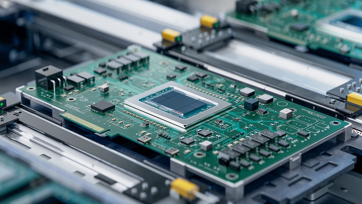
Lithography is the most important processing technology of integrated circuits and the most critical technology for manufacturing chips. In the entire chip manufacturing process, the implementation of almost every process is inseparable from the technology of lithography.
What is a Mask Aligner?
Mask Aligner is one of the core equipment of wafer manufacturing, which can be divided into several types according to the purpose: there are lithography machines for producing wafers. There are lithography machines for packaging, and there are projection lithography machines in the field of LED manufacturing. The world produces tens of billions of mobile phone chips and memory every year. For decades, they have relied on the exposure and development process with complicated procedures, but the principle is like that of developing photos.
How Does Mask Aligner Work?
The light from the photolithography machine is used to expose the sheet coated with photoresist through a photomask with a pattern, and the photoresist will change its properties. When exposed to light the pattern on the photomask is copied to the sheet so that the sheet has electronic circuits the role of the graph. This is what photolithography does, like taking pictures with a camera. The photos taken by the camera are printed on the negative, and photolithography engraves not the photos, but the circuit diagrams and other electronic components. To put it simply, a lithography machine is an enlarged SLR, and a lithography machine is to print the designed integrated circuit pattern on the mask on the photosensitive material through the exposure of light to form a pattern.
In the process of processing the wafer, the lithography machine transmits the light beam through a mask with a circuit diagram through a series of light source energy and shape control methods, compensates various optical errors through the objective lens, and scales the circuit diagram and maps it to the silicon. The chip is developed using chemical methods to obtain a circuit diagram engraved on the silicon wafer. The general lithography process needs to go through the steps of cleaning and drying the surface of the silicon wafer, coating, spin coating photoresist, soft baking, alignment exposure, post-baking, developing hard braking, and laser etching. After one photolithography, the wafer can continue to be glued and exposed. The more complex the wafer, the more layers of the circuit pattern, and the more precise the exposure control process is required.
What Structures and Objects Does Mask Aligner Have?
- Measuring table, exposure table: It is a work table that carries silicon wafers.
- Laser: The light source, one of the core equipment of the lithography machine.
- Beam Corrector: Correct the incident direction of the beam to make the laser beam as parallel as possible.
- Energy controller: Controls the energy that is finally irradiated on the silicon wafer. Underexposure or overexposure will seriously affect the image quality.
- Beam shape setting: Set the beam to different shapes such as circles, rings, etc. Different beam states have different optical properties.
- Shutter: Blocks the beam from reaching the wafer when exposure is not required.
- Energy detector: Detect whether the final incident energy of the beam meets the exposure requirements, and feed it back to the energy controller for adjustment.
- Reticle: A glass plate with wiring diagrams engraved on the inside, which can cost hundreds of thousands of dollars.
- Mask stage: The device that carries the movement of the reticle, and the movement control precision is nm level.
- Objective lens: The objective lens is used to compensate for optical errors and to scale down the circuit diagram.
- Silicon Wafer: A wafer made of silicon wafers. Silicon wafers come in a variety of sizes, and the larger the size, the higher the yield. As a digression, since the silicon wafer is round, it is necessary to cut a notch on the silicon wafer to confirm the coordinate system of the silicon wafer. According to the shape of the notch, it is divided into flat or notch.
- Internal closed frame, shock absorber: Isolate the workbench from the external environment, keep it level, reduce external vibration interference, and maintain stable temperature and pressure.
What are the Important Indicators of Lithography Technology?
- Lens:
The lens is the core part of the lithography machine. It is not an ordinary lens. It can reach a height of 2 meters and a diameter of 1 meter, or even larger. The entire exposure optical system of the lithography machine is composed of dozens of mirrors with large pot bottoms in series, and the precision of the optical parts is controlled within a few nanometers.
- Light source:
The light source is one of the cores of the lithography machine, and the process capability of the lithography machine first depends on the wavelength of its light source. The light source of the earliest lithography machine is the UV light source (Ultraviolet Light) produced by a mercury lamp, which has been developed from g-line to i-line, and the wavelength is reduced to 365nm, and the actual corresponding resolution is about 200nm or more. Subsequently, the industry adopted the DUV light source (Deep Ultraviolet Light) of excimer laser. The wavelength was further narrowed down to 193 nm for ArF. However, after the 157nm F2 excimer laser that was originally planned to be used next encountered a series of technical obstacles, ArF Immersion Technology became the mainstream. Immersion technology involves immersing the space between the lens and the silicon wafer in liquid. Since the refractive index of the liquid is greater than 1, the actual wavelength of the laser will be greatly reduced. The refractive index of pure water currently used in the mainstream is 1.44, so the actual equivalent wavelength of ArF plus immersion technology is 193nm/1.44=134nm. resulting in higher resolution.
- Resolution:
The Resolution of the lithography machine represents the ability of the lithography machine to project the smallest image, which is one of the most important technical indicators of the lithography machine and determines the level of process nodes that the lithography machine can be applied. But it must be noted that although the resolution and the wavelength of the light source are closely related, the two are not completely corresponding.
- Overlay accuracy:
The basic meaning of overlay accuracy refers to the alignment accuracy (3σ) of the patterns between the two lithography processes before and after. If the alignment deviation is too large, it will directly affect the product yield. For high-end lithography machines, general equipment suppliers will provide two values for the overlay accuracy, one is the double overlay error of a single machine itself, and the other is the overlay error between different devices. Overlay accuracy is another important technical indicator of the lithography machine.
- Nodes:
Nodes are the most direct parameters reflecting the technological level of integrated circuits. The current mainstream nodes are 0.35um, 0.25um, 0.18um, 90nm, 65nm, 40nm, 28nm, 20nm, 16/14nm, 10nm, 7nm, etc. Traditionally, the value of the node generally refers to the minimum length (gate length) of the gate of the MOS transistor, and the minimum pitch of the second metal layer (M2) wiring is used as the node index.



.jpg)
