The Foundation of The Semiconductor Industry: Wafer
Knowledge

The Foundation of The Semiconductor Industry: Wafer

When reading or hearing about the semiconductor industry, we often hear the term wafer mentioned. But what exactly is a so-called wafer? What does an “8 inch” or “12 inch” wafer refer to? How difficult is it to produce large-sized wafers? The following is a step-by-step introduction to the most important foundation of semiconductors, the wafer.
Published: Jun 20, 2022
The Foundation of The Semiconductor Industry: Wafer

What is a Wafer?

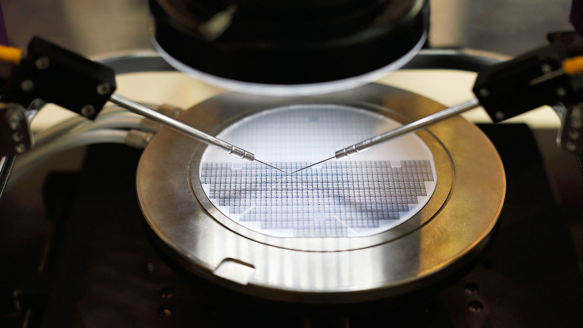
A wafer refers to the silicon wafer used in the fabrication of silicon semiconductor integrated circuits. Because of its circular shape, it is called a wafer. A wafer is the carrier used in the production of integrated circuits. Generally, a wafer refers to a single-crystal silicon wafer. Wafers are the most commonly used semiconductor base material, and are divided into 4 inches, 5 inches, 6 inches, and 8 inches according to their diameters. The larger the wafer, the more ICs can be produced on the same wafer, which can reduce costs. However, the requirements for material technology and production technology are higher for larger wafers. It is generally believed that the larger the diameter of the silicon wafer, the better the technology of the fab. In the process of producing wafers, the yield rate is a very important condition.

Wafers are the basis for the manufacturing of computer chips. We can compare chip manufacturing to building a house with Lego blocks, and by stacking layer by layer, we can complete our desired shape (that is, the desired chip). However, if there is no good foundation, the built house will be deformed and unsatisfactory. In order to make a perfect house, a stable base plate is required. For wafer fabrication, this substrate is the wafer described next.

I recall that when I was a child with Lego blocks, there would be small round protrusions on the surface of the blocks. With this structure, we can stably stack the two blocks together without using glue. Wafer fabrication, in a similar way, holds the subsequently added atoms together with the substrate. Therefore, we need to find substrates with neat surfaces to meet the conditions required for subsequent fabrication.

In solid materials, there is a special crystal structure - Monocrystalline. It has the property of atoms closely arranged one after the other, forming a flat atomic surface. Therefore, using a single crystal to make a wafer can meet the above requirements. However, to produce such a material, there are two main two steps, purification and crystal pulling.

How to Make a Single Crystal Wafer?

Purification is divided into two stages. The first step is metallurgical purification. This process mainly involves adding carbon to silicon oxide to convert it by redox into silicon with a purity of more than 98%. Most of the refining of metals, such as iron or copper, is done in this way to obtain metals of sufficient purity. However, 98% is still not enough for wafer manufacturing and still needs to be improved further. Therefore, the Siemens process will be used for further purification, so that the high-purity polysilicon required for the semiconductor process will be obtained.

Next, is the step of pulling crystals. The previously obtained high-purity polysilicon is melted to form liquid silicon. After that, a single-crystal silicon seed contacts the liquid surface, and is slowly pulled up while rotating. The single-crystal silicon seeds are needed to initiate the order in which the silicon atoms will arrange on the crystal as it grows. Finally, after the silicon atoms leaving the liquid solidify on the surface of the crystal, the neatly arranged monocrystalline silicon pillars are completed.

However, what do 8 inches and 12 inches stand for? This refers to the diameter of the crystal column after it is completed. How difficult is it to make large wafers? As described earlier, the accumulation on the crystal is like the process of making cotton candy. As the center is rotated multiple layers are added till you get the desired diameter. If you have made cotton candy, you will appreciate that as the core gets larger it becomes harder to make a uniform end product. With the pulling of crystals, it is the same. The speed of rotation, and control of the temperature will affect the quality of the crystal column. Therefore, the larger the size, the higher the speed and temperature requirements for crystal pulling, so it is more difficult to make high-quality 12-inch wafers than 8-inch wafers.

To obtain the wafer, this silicon pillar now needs to be cut into thin slices. A diamond knife is used to cut the silicon pillars laterally into wafers, and the wafer’s surfaces are then polished to form the final completed wafers. Once the wafer substrate is complete, the next step of stacking the circuits onto the wafer will complete the chip fabrication.

Published by Jun 20, 2022 Source :Business Next

Further reading

You might also be interested in ...

Headline
Knowledge
Understanding the Logistics and Transportation Sector
As the number of e-commerce transactions continues to surge, there is a parallel increase in the demand for logistics services. Amidst the ongoing transformation and upgrade of the industry, the integration of smart technology has emerged as a pivotal factor in driving its development.
Headline
Knowledge
Understanding Mechanism Design and Its Practical Applications
Creating an effective mechanism design entails thoughtful consideration of factors such as materials, specifications, precision, manufacturing processes, and functionality. Moreover, it must be cost-effective to ensure the development of a successful mechanism design.
Headline
Knowledge
Understanding the Granulation Process
Plastic granulation technology plays a pivotal role in the manufacturing of plastic products and the recycling of resources. It is employed to produce a diverse range of plastic products or raw materials, offering both environmental and economic advantages.
Headline
Knowledge
What Constitutes Contemporary Architectural Frameworks for Robotic Computing?
The behavior of robots is frequently modeled as a computational graph, wherein data flows from sensors to computational technology, extending to actuators and then looping back. To enhance performance capabilities, robotic computing platforms need to adeptly map these graph-like structures to CPUs and specialized hardware, such as FPGAs and GPUs.
Headline
Knowledge
How Does the Electroplating Process Work for ABS Plastic?
Over the past few years, plastic electroplating has gained widespread popularity, particularly in the decorative electroplating of plastic components. Among the various types of plastic utilized in electroplating, ABS plastic stands out as the most extensively employed.
Headline
Knowledge
What Are the Fundamentals and Benefits of Choosing between Liquid and Powder Coating?
Metal fabricators aiming to venture into finishing processes should familiarize themselves with two prevalent options—liquid and powder coating—along with the prerequisites necessary for a company seeking to employ either or both.
Headline
Knowledge
Anticipating the Emerging Trends in the Global Laser Industry
In light of the evolving global industry demands, the laser industry and technology are shifting their focus towards meeting the requirements of 5G semiconductors and smart vehicle processes. While Taiwan's laser industry has a well-established foundation built over the years, sustaining international competitiveness necessitates a proactive advancement in independent laser technology.
Headline
Knowledge
What is the Purpose of Surface Treatment for Metals?
Defects are bound to arise during the reprocessing of mechanical equipment or parts related to metal. As a result, the final item's surface treatment process plays a crucial role, serving the dual purpose of enhancing aesthetics and providing protection. This process not only improves the performance of metal parts but also helps prevent rust.
Headline
Knowledge
Selecting a Hydraulic Press and Understanding its Manufacturing Procedure
Hydraulic presses find applications in compaction, assembly, pressing, forming, embossing, and stretching. They play a crucial role in compaction within the cosmetics sector, assembly in the automotive industry, molding of electronic products, and stamping in the home appliance industry.
Headline
Knowledge
Introduction to RFID Tags: The Significance of RFID in Modern Retail Supply Chains
There are two types of RFID systems: passive and active. For those unfamiliar with RFID, you may be curious about the distinctions between these types and which one suits your application best. In the following, we offer a brief explanation.
Headline
Knowledge
Anticipating the Emerging Trends in the Global Laser Industry
In light of the evolving global industrial demands, the laser industry and technology are shifting towards meeting the requirements of 5G semiconductors and advanced processes for smart vehicles. While Taiwan's laser industry has made substantial progress over the years, maintaining alignment with international advancements necessitates a proactive push in independent laser technology.
Headline
Knowledge
Exploring Sheet Metal: Defining Sheet Metal and its Various Applications, with a Focus on Laser Applications
The term originates from English, known as plate metal. Typically, certain metal sheets undergo plastic deformation either manually or through die-stamping to attain the desired shape and size. These sheets can then undergo additional shaping through welding or a limited amount of mechanical processing to create more intricate components.
Agree