Taiwan's semiconductor industry is booming, and sub-industries such as wafer foundry, back-end packaging, and testing, and IC design are among the best in the world.
The Industry Classification of the Semiconductor Industry:
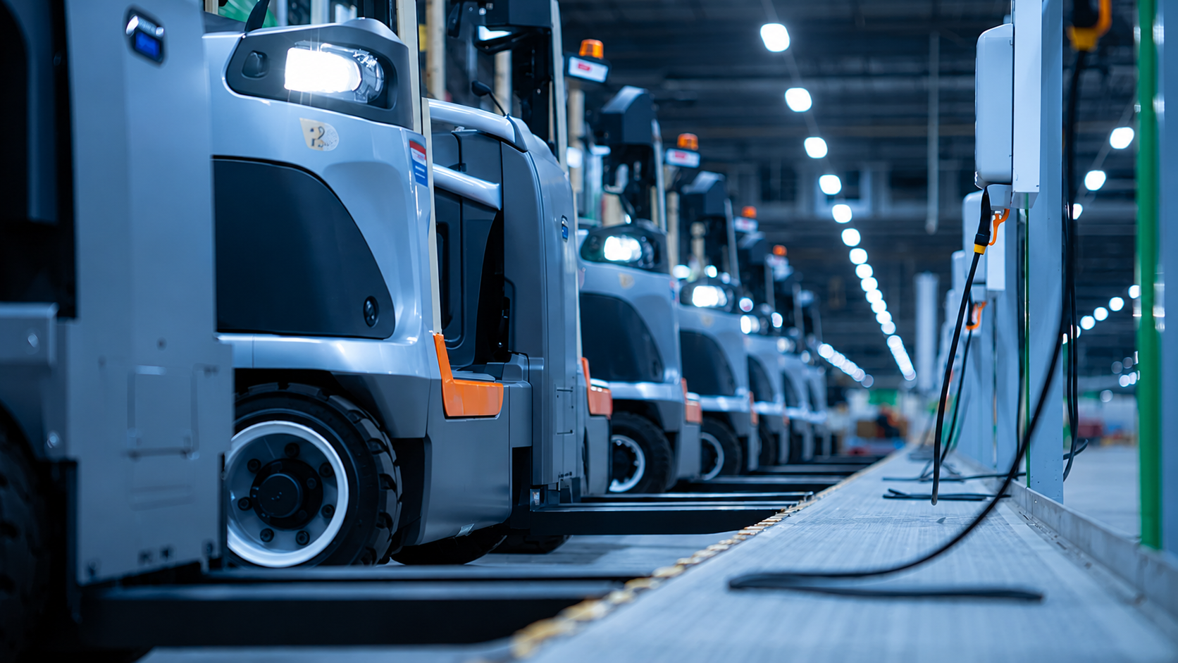
Semiconductor equipment can be divided into semiconductor process equipment, semiconductor packaging equipment, peripheral equipment for a semiconductor process, and semiconductor testing equipment.
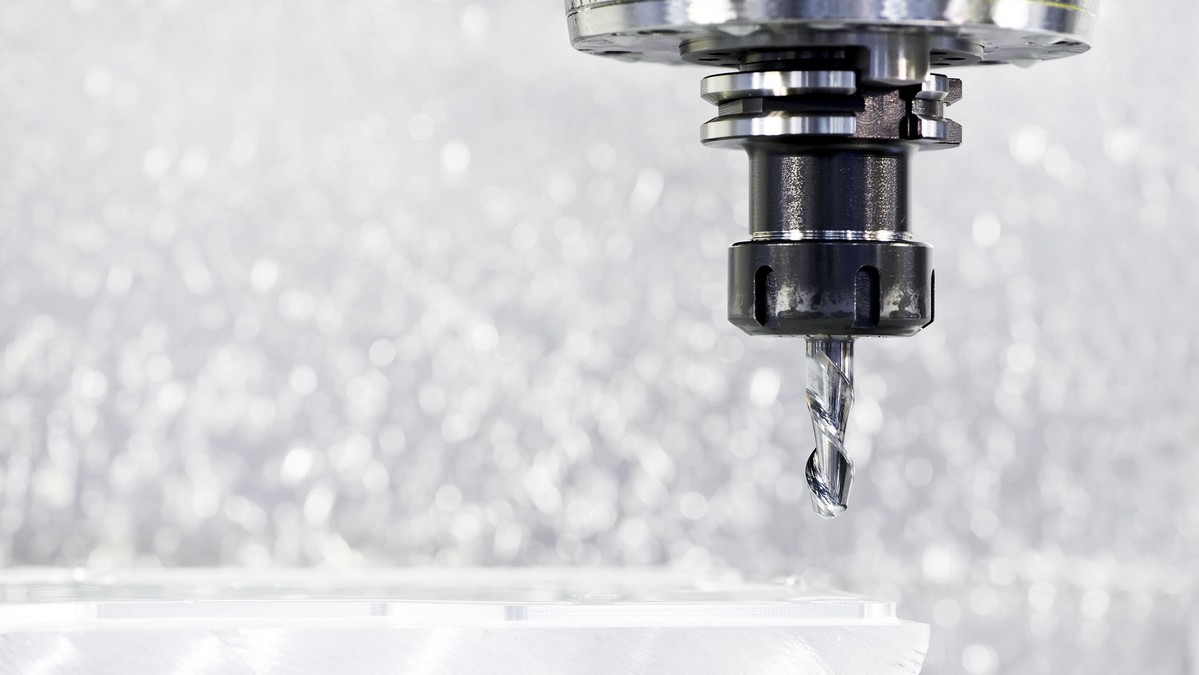
- Semiconductor process equipment and parts: Machines, equipment, or devices used in the manufacturing process of the semiconductor industry. The scope includes equipment required for oxidation, diffusion, deposition, lithography, etching, evaporation, and other processes.
- Semiconductor packaging equipment and parts: Machines, equipment, or devices used in the assembly process of the semiconductor industry. The scope includes the equipment required for wafer cutting, grinding, die bonding, wire bonding, sealing, molding, stamping, etc.
- Peripheral equipment and parts for semiconductor process: Peripheral-related equipment used in the semiconductor process. The scope includes related factory equipment such as pure water, clean room, precision automatic valve, and ultra-precision machining pipe fittings in the process.
- Semiconductor testing equipment and parts: Machines, equipment, or devices used in the inspection process of the semiconductor industry. The scope includes equipment required for logic, linear, memory, needle testing machines, sorting machines, etc.
What Processes and Equipment are there in the Semiconductor Industry?
Semiconductor equipment generally refers to the production equipment required to produce various semiconductor products and belongs to the key supporting link of the semiconductor industry chain. Semiconductor equipment is the technological leader in the semiconductor industry. Chip design, wafer manufacturing, and packaging and testing must be designed and manufactured within the scope of equipment technology. The advancement of equipment technology also promotes the development of the semiconductor industry.
Taking the integrated circuit with the highest technical difficulty, the largest added value, and the most complex process in the semiconductor industry chain as an example, the equipment used in the field of integrated circuits can usually be divided into front-end process equipment (wafer manufacturing) and back-end process equipment (packaging and testing).
Front-end Process Equipment (Wafer Fabrication):
The seven major steps in front-end wafer fabrication are oxidation/diffusion, lithography, etching, cleaning, ion implantation, film growth, and polishing. The semiconductor equipment used in each step is as follows:
- Oxidation/diffusion/annealing process:
- Oxidation procedure and oxidation furnace:
Oxidation is a process in which a silicon wafer is placed in an atmosphere of an oxidant such as oxygen or water vapor for high-temperature heat treatment, and a chemical reaction occurs on the surface of the silicon wafer to form an oxide film. It is an indispensable part of the semiconductor processing process to provide the required oxidizing atmosphere for the oxidation treatment of semiconductor materials and realize the oxidation treatment expected by the semiconductor design.
- Diffusion Procedure and Diffusion Furnace:
Diffusion refers to doping impurity elements into the silicon substrate according to the process requirements by using the principle of thermal diffusion under high-temperature conditions, so that it has a specific concentration distribution, thereby changing the electrical properties of the silicon material. Diffusion furnaces are used for diffusion, oxidation, annealing, alloying, and sintering processes in industries such as large-scale integrated circuits, discrete devices, power electronics, optoelectronic devices, and optical fibers. The main purpose of the diffusion process is to dope semiconductor wafers under high-temperature conditions, that is, to diffuse the elements phosphorus and boron into the silicon wafer, thereby changing and controlling the type, concentration, and distribution of impurities in the semiconductor to establish regions of different electrical characteristics.
- Annealing procedure and annealing furnace:
Annealing refers to the process of heating the silicon wafer after ion implantation and repairing the lattice defects caused by ion implantation. Process equipment used in the manufacture of semiconductor devices involves heating a plurality of semiconductor wafers to affect their electrical properties. Heat treatments are designed for different effects. The wafer can be heated to activate dopants, convert thin films to thin films or convert thin films to wafer substrate interfaces, densify deposited thin films, change the state of growing thin films, repair implanted damage, move dopants or transfer dopants the agent is transferred from one film to another or from the film into the wafer substrate.
- Photolithography process:
The main process in the production of planar transistors and integrated circuits is a processing technology for opening the mask on the surface of the semiconductor wafer for the localized diffusion of impurities. The general lithography process needs to go through such processes as cleaning and drying the surface of the silicon wafer, priming, spin-coating photoresist, soft baking, alignment exposure, post-baking, developing, hard baking, etching, and testing.
- Glue coating and developing equipment:
The glue coating and development equipment uses the robot to realize the transfer and processing of the wafer between the various systems and achieves perfect cooperation with the photolithography machine to complete the photoresist coating, curing, and development of the wafer. As the input of the photolithography machine, that is, the photoresist coating before exposure, and the output. The development of the pattern after exposure, the performance of the coating and developing machine not only directly affects the formation of fine exposure, but also the pattern quality and error control of the development process. It also has a profound impact on the pattern transfer results in the subsequent etching and ion implantation processes.
- Lithography equipment:
Mask align is the core equipment for manufacturing wafers. It uses a technique like photo printing to print the fine patterns on the mask onto the silicon wafer through exposure to light. The lithography machine is the core equipment to produce large-scale integrated circuits, which requires the mastery of profound optical and electronic industry technologies.
- Alignment detection equipment:
The alignment detection equipment is mainly used for the alignment of the mask and the wafer in the lithography process, the alignment of the wafer and the substrate when the wafer is bonded, and the alignment of the components and the PCB substrate in the surface assembly process. It is also used in various processing processes. Among them, such as wafer testing, wafer dicing, various laser processing processes, etc. Precision detection technology is the basis of alignment detection, and detection methods mainly include optical detection methods and photoelectric detection methods.
Back-end Process Equipment (Package Test):
Semiconductor packaging and testing is an extremely important finishing touch in the semiconductor manufacturing process. Semiconductor packaging is a process in which chips are laid out, fixed, and connected on a substrate using technologies such as thin-film microfabrication, and then potted with a plastic insulating medium to form electronic products. The purpose is to protect the chip from damage, ensure the heat dissipation performance of the chip, and realize the power and the transmission of electrical signals to ensure the normal operation of the system; semiconductor testing is mainly to test the appearance and performance of the wafer, the purpose is to ensure product quality. Specifically, the main semiconductor packaging and testing equipment include:
- Thinner:
Due to the requirements of the manufacturing process, high requirements are placed on the dimensional accuracy, geometric accuracy, surface cleanliness, and surface micro lattice structure of the wafer. Therefore, in the process flow, only wafers with a certain thickness can be used for transfer and tape-out in the process. Usually, the excess substrate material on the backside of the wafer needs to be removed by a thickness before IC packaging. This process is called the wafer backside thinning process, and the corresponding equipment is a wafer thinning machine. The thinning machine thins the wafer substrate by thinning/grinding to improve the heat dissipation effect of the wafer. Thinning to a certain thickness is beneficial to the later packaging process.
- Dicing machine:
There are two types of dicing machines: grinding wheel dicing machines and laser dicing machines. Among them, the grinding wheel dicing machine is a precision numerical control equipment that integrates the technologies of water, gas, electricity, air static pressure high-speed spindle, precision mechanical transmission, sensors, and automatic control. Mainly used for dicing and processing of silicon integrated circuits, light-emitting diodes, lithium niobate, piezoelectric ceramics, gallium arsenide, sapphire, alumina, iron oxide, quartz, glass, ceramics, solar cells, and other materials. The laser dicing machine uses a high-energy laser beam to irradiate the surface of the workpiece so that the irradiated area is partially melted and vaporized, to achieve the purpose of dicing. Because the laser is focused by a special optical system to become a very small spot, the energy density is high, and because the processing is non-contact, there is no mechanical punching force on the workpiece itself, and the workpiece is not easily deformed. The thermal influence is extremely small and the scribing accuracy is high. It is widely used in the cutting and scribing of solar panels and thin metal sheets.
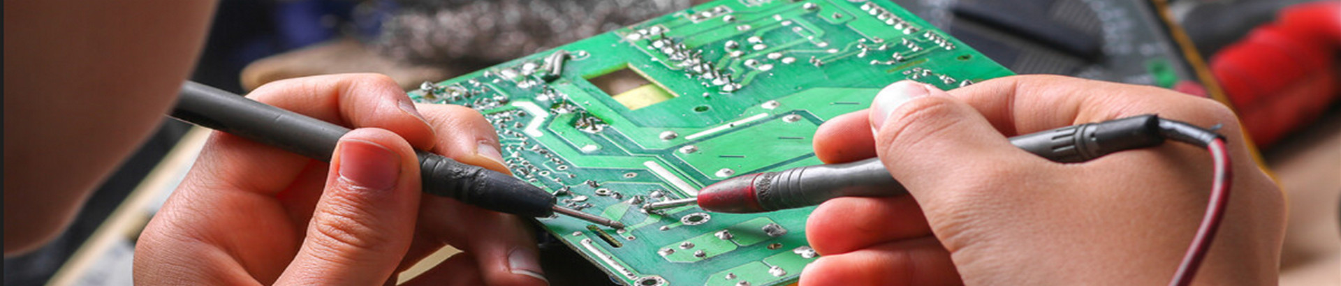
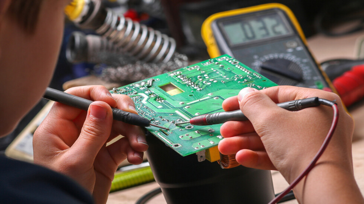
- Test machine:
The tester is special equipment for testing the function and performance of the wafer. During the test, the tester applies an input signal to the wafer to be tested and compares the obtained output signal with the expected value to judge the electrical performance of the wafer and the effectiveness of the product function. In the CP and FT testing links, the testing machine transmits the results to the probe station and the sorter respectively. When the probe station receives the test results, an inkjet operation is performed to mark defective chips on the wafer. When the sorter receives the results from the tester, it selects and sorts the wafers.
- Sorter:
The sorting equipment is used in the FT test link after the chip packaging. It is a back-end test equipment that provides the functions of chip screening and classification. The sorting machine is responsible for transporting the input chips to the test module according to the pick-and-place method designed by the system to complete the circuit pressure test. In this step, the sorting machine selects and classifies the circuits according to the test results. The sorting machine can be divided into gravity sorting machine, turret sorting machine and pick and place sorting machine according to the system structure.
- Probe machine:
The probe station is used for the CP test link after wafer processing and before the packaging process. It is responsible for the transportation and positioning of the wafer so that the dies on the wafer are sequentially contacted with the probe and tested one by one. The workflow of the probe station is to move the wafer under the wafer camera through the wafer stage, capture the wafer image through the wafer camera, determine the position of the wafer, and move the probe camera under the probe card. Determine the position of the probe head, then move the wafer under the probe card, and realize the needle alignment through the vertical movement of the slide table.
Characteristics of Taiwan's Semiconductor Equipment Industry:
- Regional effects of semiconductor equipment manufacturers:
Equipment manufacturers in the north account for 76% of the total. The main reason is that most of the semiconductor manufacturers are in Hsinchu. To serve customers nearby, most equipment manufacturers choose to set up factories in the northern region.
- Semiconductor equipment manufacturers are mainly small and medium-sized enterprises:
Domestic equipment manufacturers have less than 50 employees, accounting for 67% of all equipment manufacturers, indicating that Taiwan's semiconductor equipment industry is dominated by small and medium-sized enterprises.
- The domestic demand for semiconductor equipment is far greater than the output value:
The output value is lower than the market demand, indicating that domestic equipment manufacturers have considerable development potential.
- The sales of domestic semiconductor equipment are mainly domestic:
Taiwan's domestic semiconductor industry is developing vigorously, and the market demand for semiconductor equipment is far greater than the domestic output value. Therefore, the marketing area of Taiwan's semiconductor equipment manufacturers is mainly domestic, and a few are sold abroad.
- Semiconductor equipment manufacturers do not have the technology to produce key equipment:
Taiwanese equipment manufacturers mainly produce back-end equipment, and the technical level of the front-end process is relatively high. At present, Taiwanese domestic manufacturers still cannot produce such key equipment.
- High industrial relevance:
The manufacturing process of semiconductor, photovoltaic, and LED industries are similar. The development of Taiwan's semiconductor equipment industry can also support the LED and photovoltaic equipment industries at the same time.