This article examines the role of double column high-speed graphite machine centers in semiconductor manufacturing. It explores graphite's properties—high-temperature resistance, purity, and thermal conductivity—that make it essential for wafer processing and crystal growth components. The article details machining challenges and how the SD1000G machine center addresses them with high-speed spindles, precision positioning, dust containment, and thermal stability for semiconductor-grade production.
The Strategic Role of Graphite in Semiconductor Manufacturing
In the rapidly evolving landscape of semiconductor manufacturing, precision and purity are not merely objectives—they are absolute requirements. As the industry pushes toward smaller nodes and more demanding applications, the materials and processes used in wafer fabrication equipment, crystal growth systems, and thermal management components must meet increasingly stringent standards. Graphite has emerged as an indispensable material in this ecosystem, and the machines that shape it have become critical enablers of semiconductor innovation.
Graphite's unique combination of properties makes it invaluable across multiple semiconductor applications. Isostatic graphite, in particular, has gained prominence due to its uniform structure, exceptional purity, and superior mechanical and thermal performance. It can withstand extreme temperatures—often exceeding 3000°C in inert environments—while maintaining structural integrity, a capability essential for crystal growth processes and high-temperature furnaces. Its high purity levels are equally critical, as even trace contamination can compromise the delicate processes involved in semiconductor fabrication. The semiconductor industry's reliance on high-purity graphite components has been growing steadily, with applications ranging from wafer processing equipment and heating elements to susceptors and crystal growth components.
In recent years, significant advances have been made in developing ultra-pure, ultra-fine graphite materials specifically for semiconductor applications. For instance, isostatic graphite can be manufactured to achieve impurity levels of <1 ppm, ensuring compliance with stringent semiconductor and high-tech industry standards. These materials must maintain dimensional stability at near-3000°C temperatures without introducing any contamination to the crystal growth process. The thermal management challenges in modern electronics have further expanded graphite's role, as its excellent thermal conductivity and low thermal expansion make it ideal for demanding processes involving rapid heating and cooling cycles.
Why Semiconductor Graphite Components Demand Specialized Machining
The components used in semiconductor manufacturing are not simple graphite blocks. They require intricate geometries, tight tolerances, and exceptionally clean surfaces. Whether producing susceptors for epitaxial growth, ion implant hardware, or sputtering targets, the machining process must deliver precision while addressing the unique challenges graphite presents.
Graphite is inherently brittle and abrasive. Traditional machining approaches often result in edge chipping, dimensional inaccuracies, and excessive tool wear. Furthermore, graphite dust—a byproduct of the machining process—poses significant risks. The dust can infiltrate precision machine components such as guideways and ball screws, accelerating wear and compromising long-term accuracy. In semiconductor applications, where contamination must be controlled at the parts-per-billion level, effective dust management becomes paramount. The need for dust containment has driven the development of specialized machining centers with features such as strong negative-pressure dust suction systems and full-guard enclosures to prevent dust leakage.
Moreover, the trend toward ultra-fine and ultra-pure graphite materials introduces additional challenges. Premium graphite grades with average particle sizes of less than 5 microns offer high strength and resistance to damage, but they require precise machining techniques to achieve the fine surface finishes necessary for semiconductor applications. These challenges necessitate machining solutions specifically engineered to handle the material's unique characteristics while maintaining the clean environment required for semiconductor-grade components.
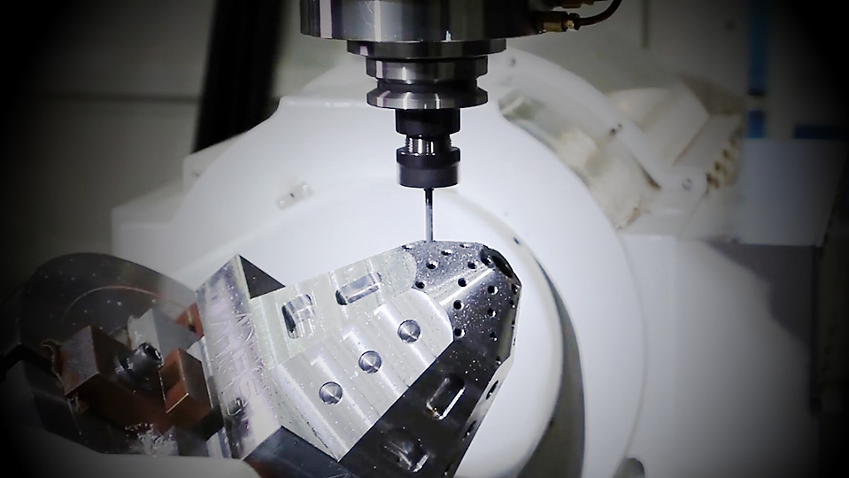
The Double Column High-Speed Graphite Machine Center: A Targeted Solution
The double column high-speed graphite machine center addresses these challenges through a combination of structural design and application-specific engineering. This machine type has become the preferred solution for manufacturers serving the semiconductor industry, offering capabilities specifically aligned with the demanding requirements of graphite component production.
Rigidity and Stability for Precision
The double column design provides exceptional structural rigidity and stability. This configuration, with its integral column and wide base, effectively suppresses vibration during machining—a critical factor when working with graphite's brittle nature. As industry research indicates, double column structural designs can reduce the vibration effect in high-speed machining, improve contour accuracy, and result in superior surface finishing on workpieces, while also extending tool service life. The enhanced rigidity enables consistent cutting performance even during rapid feed rates and complex 3D contouring operations.
High-Speed Machining for Efficiency and Quality
High-speed spindle technology is essential for efficient graphite machining. By operating at elevated speeds with appropriate torque characteristics, the machine achieves "light cutting, fast feed" conditions that minimize cutting resistance. Advanced built-in motorized spindles with speeds up to 30,000 rpm are commonly employed for high-speed machining applications, presenting high cutting rates, low vibration, and better axial and radial rigidity. This approach offers multiple benefits:
- Extended tool life: Reduced cutting forces decrease the risk of tool edge chipping, a common problem when machining graphite.
- Improved surface quality: Higher speeds enable finer surface finishes directly from the machine, often reducing or eliminating the need for subsequent hand polishing.
- Increased throughput: Faster machining cycles translate to higher productivity and shorter lead times for critical semiconductor components.
Essential Features for Semiconductor-Grade Machining
When evaluating a graphite machining center for semiconductor applications, specific technical features become decisive factors:
- Dust Containment Systems: Effective dust control is non-negotiable for semiconductor applications. The machine must feature a fully enclosed working area with a robust negative-pressure dust extraction system. Features such as vacuum internal spaces, dry cutting systems, and strong negative dust suction with close full guards are essential to prevent dust leakage and protect both operator health and machine precision components.
- Thermal Management: High-speed operation generates heat that can cause thermal expansion and compromise positioning accuracy. Advanced machines incorporate oil cooling systems and spindle thermal compensation to maintain consistent accuracy during extended production runs. Additionally, guideway covers on all axes and central auto-oil lubrication systems help protect critical components from contamination and thermal distortion.
- High-Precision Motion Control: The ability to execute complex tool paths with precision requires high-performance servo systems and responsive controls. The machine must support high acceleration and deceleration rates while maintaining positional accuracy—capabilities essential for the intricate geometries found in semiconductor components.
Semiconductor-Grade Graphite Machining Solution: SD1000G
For semiconductor graphite component manufacturing, the SD1000G Double Column High-Speed Graphite Machine Center incorporates the following key design features:
- High-speed spindle system: Equipped with a high-speed spindle (up to 30,000 rpm) and HSK tool interface, enabling a "light cutting, fast feed" approach that effectively reduces burrs and edge chipping on graphite electrodes and thin-wall components
- Precision positioning and rigidity: Double column structure provides excellent rigidity and vibration resistance, with positioning accuracy of ±0.005 mm to meet critical dimensional requirements for susceptors, ion implant hardware, and similar components
- Full-enclosure dust collection: Fully enclosed guarding with a powerful negative-pressure dust extraction system effectively contains graphite dust, protecting guideways and ball screws while maintaining process cleanliness
- Thermal stability control: Spindle oil cooling system with thermal compensation ensures machining accuracy stability during extended high-speed operation
Note: Please refer to the official technical specification sheet for actual travel, tool magazine capacity, spindle power, and controller details.
Meeting the Evolving Standards of the Semiconductor Industry
The semiconductor sector demands more than just capable equipment; it requires traceability, reliability, and a commitment to quality that aligns with the industry's exacting standards. A machine center designed for semiconductor graphite processing represents an investment not just in production capacity but in the ability to meet the evolving needs of a demanding market.
As semiconductor technology continues to advance—with the emergence of wide-bandgap materials like SiC and GaN, the increasing complexity of chip architectures, and the growing demands of high-power and high-frequency applications—the role of precision-machined graphite components will only expand. Industry leaders in the semiconductor space, including companies specializing in power semiconductors, SiC substrates, and semiconductor equipment, rely on high-quality graphite components for etching, PVD, oxidation, diffusion, and cleaning processes.
The machines that produce these components must evolve in parallel, incorporating new capabilities to address emerging requirements. For example, in monocrystalline silicon manufacturing equipment, graphite products must withstand melting temperatures of approximately 1500°C while maintaining dimensional stability and purity. Similarly, in silicon epitaxial growth processes, SiC-coated graphite susceptors require exceptional dimensional precision and surface roughness control to ensure proper wafer temperature distribution.
Advanced surface treatments and coatings have become increasingly important for semiconductor graphite components. SiC-coated graphite products offer excellent thermal durability, chemical resistance, dust resistance, and oxidation resistance, making them ideal for challenging environments where uncoated graphite would suffer from corrosion or particle generation. The ability to machine these coated components with precision—often to thicknesses of 0.1 mm or less—requires machine centers capable of maintaining tight tolerances while working with both the substrate and the coating material.
Conclusion: A Strategic Investment in Semiconductor Manufacturing Capability
The double column high-speed graphite machine center has established itself as a vital tool in the semiconductor manufacturing supply chain. By combining structural rigidity, high-speed machining capability, and application-specific engineering features, these machines enable the production of the high-quality graphite components essential for modern semiconductor fabrication.
For manufacturers serving the semiconductor industry, selecting a machining partner with demonstrated expertise in graphite processing is a strategic decision. The technical challenges are significant, and the cost of failure—whether through contamination, dimensional inaccuracies, or production delays—is measured in more than just dollars. A machine center designed and built with semiconductor applications in mind offers the reliability, precision, and performance that this demanding industry requires.


.jpg)